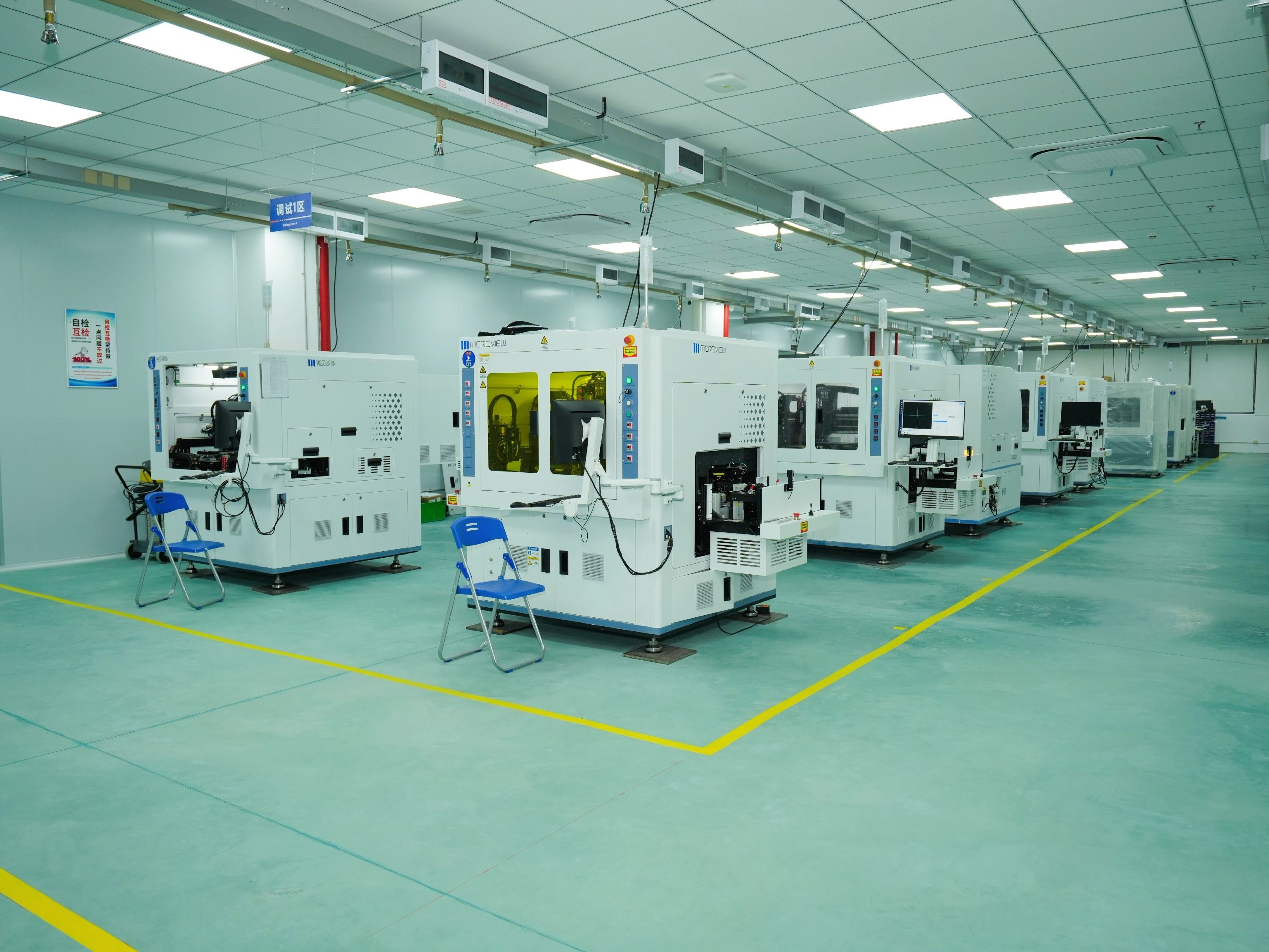
Founded in 2019, Microview is a national-level specialized and sophisticated "Little Giant" enterprise focused on the R&D and manufacturing of high-precision, complex-process chip packaging equipment, dedicated to providing advanced packaging equipment and systematic solutions to global semiconductor and pan-semiconductor customers.
Microview boasts a globally leading product portfolio covering high-precision die bonders, eutectic bonders, 3D ultra-thin stacking die bonders, flip chip bonders, TCB bonders, aligners, and die sorters. Our solutions comprehensively support 2D/2.5D/3D packaging processes and applications including COB, COC/COS, CPO/OIO, SiP, Flip-Chip, Fan-out, CoWoS/CoPoS, HBM, Stack Die, GOLD BOX, AOC/COB, and RF/Hybrid Device; chip bonding technologies such as dispensing/dipping, eutectic, sintering, reflow soldering, thermo-compression bonding, ultrasonic bonding, and laser-assisted bonding; packaging requirements for third-generation semiconductors (GaN, SiC) and high-power devices; and processes including high-precision dual-lens aligning, dual-FA aligning, CPO Lens and FAU aligning, and Automated silicon photonic chip testing. Supporting fully automated production lines, our equipment is widely applied in high-end chip packaging across Optical Communication, Storage Industry, GPU/CPU, LiDAR, RF/microwave, Commercial Lasers, AR/VR, Infrared, MEMS, CIS, and many other industries.
Microview will continue to advance its three core strategies — "Product Leadership\ Efficiency Driven\Global Marketplace" — and Committed to becoming a world-class manufacturer of high-end chip packaging equipment.